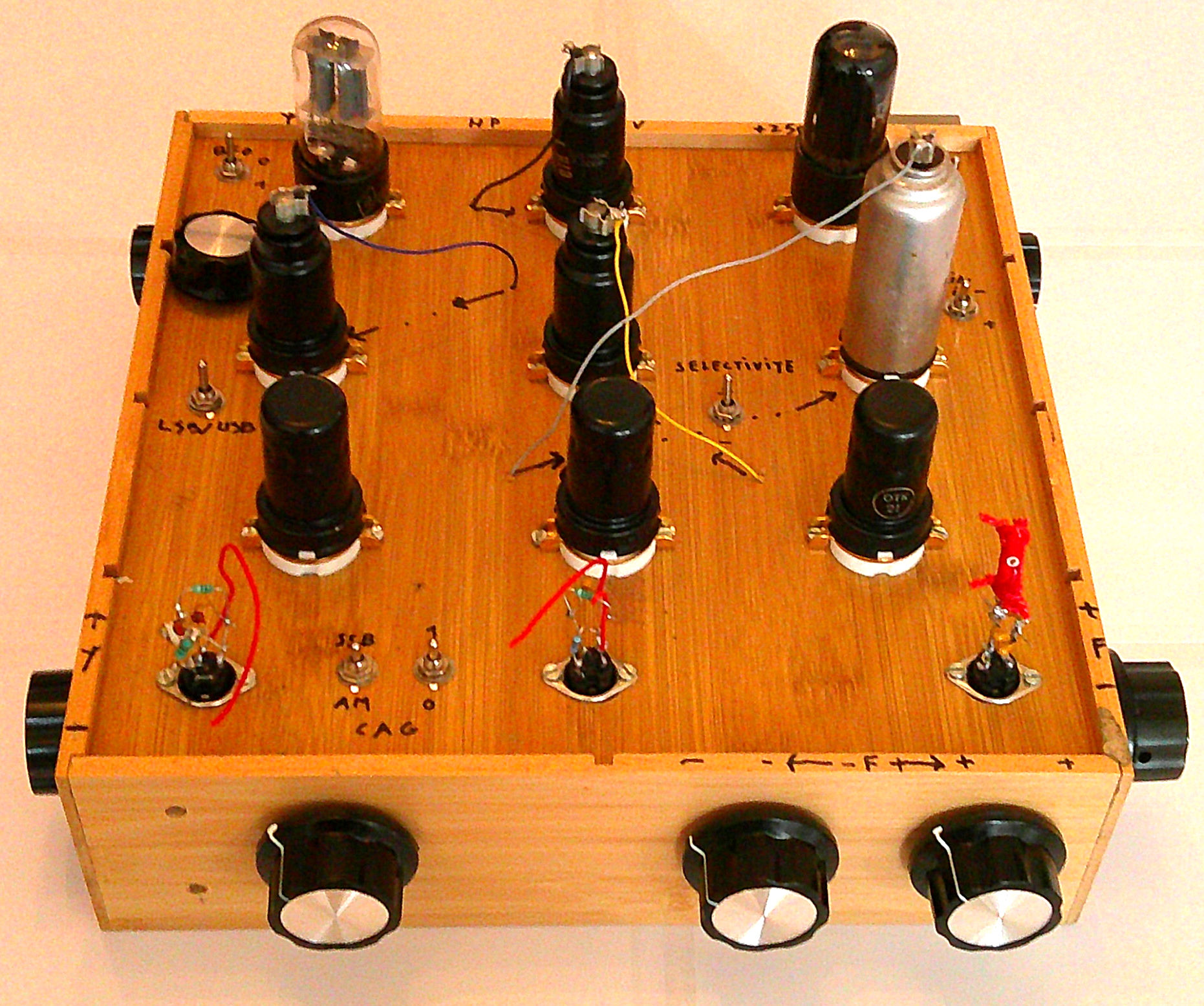
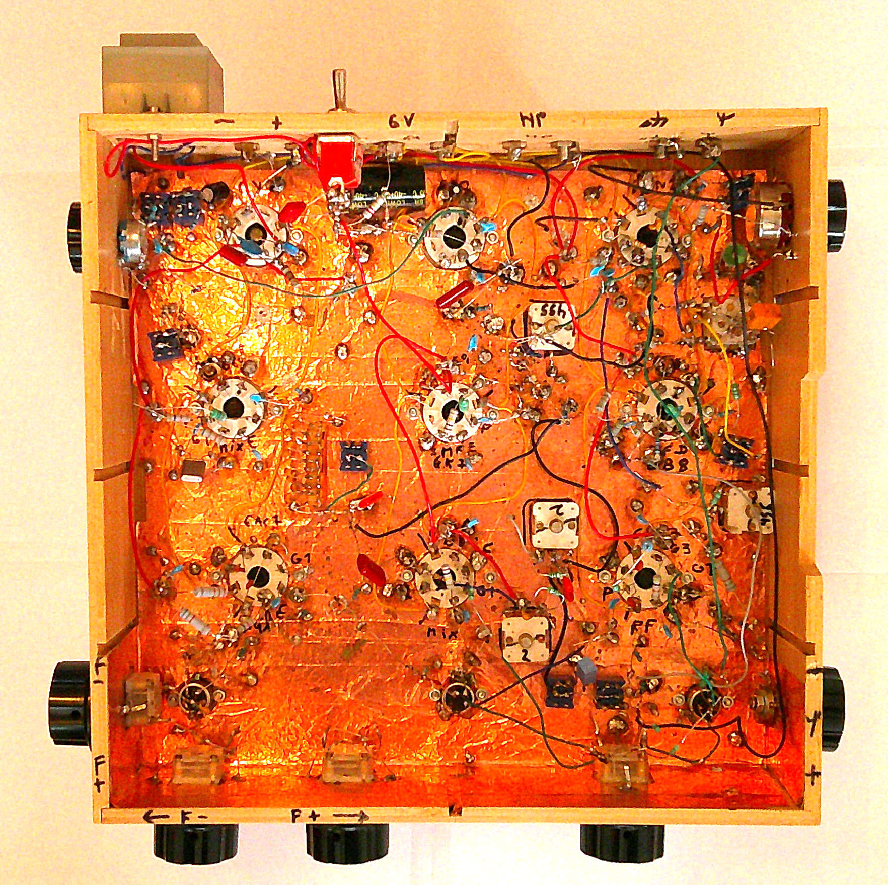
Octal-Tube Shortwave Receiver: Between Tradition and Modernity
This is a description of a tube-based shortwave (SW) receiver specifically designed for the amateur radio bands. Its design also allows other coils to be fitted, making it suitable for receiving AM broadcast stations.
The Inspiration: Classic Designs of the 1960s
The design was inspired by the HBR receivers described in QST, particularly the homebrew double-conversion receivers developed by Ted Crosby, W6TC, and by the G3RKK receiver described in the July 1963 RSGB Bulletin. I retained the HBR philosophy of plug-in coils and straightforward construction, while using modern ceramic resonators for improved 455 kHz selectivity.
Both designs used a dual-conversion architecture.
A Modernized Design for Today’s Operating
Far from being a faithful copy of the past, this receiver was designed to meet the requirements of modern operating conditions. The main changes concern three key points:
Interchangeable plug-in coils: Plug-in coils replace the traditional band-change switch. This greatly simplifies the mechanical construction and RF wiring.
Increased selectivity for SSB and CW: To obtain the “Single Signal” selectivity essential for Morse and single-sideband reception, 455 kHz ceramic resonators are used.
The aesthetic and technical choice of octal tubes: The receiver uses tubes from the Octal series to give it an authentic 1940s appearance.
The Secret of High-Frequency Operation: The 6AC7 Tube
The Octal series dates back to the second half of the 1930s. Its performance generally deteriorates above 10 MHz (as with the classic 6K7, which provides no gain at 56 MHz). To overcome this limitation, this design uses a remarkable exception: the 6AC7 tube (equivalent to the 1852 and the Russian 6Ж4 or 6J4).
Originally designed for the emerging television industry, the 6AC7 is notable for:
Exceptional gain for its time, reaching 5 at 56 MHz.
A very low noise figure.
Thanks to its performance, this tube was selected for the three receiver stages operating above 10 MHz, providing adequate sensitivity on the higher HF bands.
Circuit Analysis: Stage by Stage
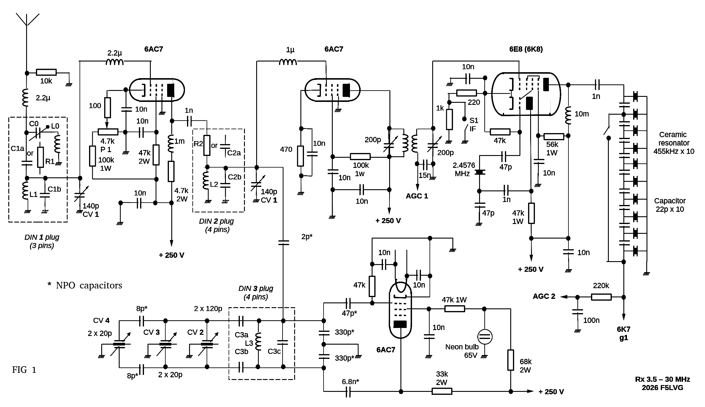
RF amplification: Provided by a first 6AC7.
Image-frequency attenuation: Two tuned circuits, adjusted by a two-section variable capacitor, provide the necessary rejection. Above 20 MHz, a series-tuned trap at the image frequency becomes essential to ensure sufficient rejection.
First frequency conversion: A second 6AC7 converts the signal to the first intermediate frequency (IF) of 2.912 MHz.
The aim is to achieve excellent frequency stability for SSB reception.
The circuit: A Colpitts oscillator built around a 6AC7. It uses a single coil with no center tap, greatly simplifying construction.
Thermal and mechanical stability:
◦ Achieved by the relatively large capacitances connecting the grid and plate to ground.
◦ The total tuning capacitance should be as high as possible (close to 1000 pF).
◦ Above 10 MHz, these high values should be obtained by paralleling fixed capacitors, each no larger than 100 pF (to limit losses and maintain oscillation).
◦ All fixed capacitors are NP0 ceramic types.
The tuning system without a mechanical reduction drive: To avoid the scarcity of mechanical reduction drives, the system uses three variable capacitors:
◦ Main tuning: To cover the entire band.
◦ Vernier: For coarse positioning.
◦ Fine tuning: Essential for precisely setting the pitch in SSB.
Frequency excursion: Ideally, the tuning range should be strictly limited to each amateur band (with a maximum of 400 kHz on 10 meters). If you do not listen to CW, restrict the tuning range to the phone portion only.
Reduced IF stage: Consisting of two miniature tuned circuits (two coils and two variable capacitors).
Second frequency conversion: Performed by a 6E8 (or 6K8) mixer tube.
Fixed oscillator: Stabilized by a 2.4576 MHz crystal. The automatic gain control (AGC) voltage is applied here to the first grid of the 6E8 (third grid for a 6K8).
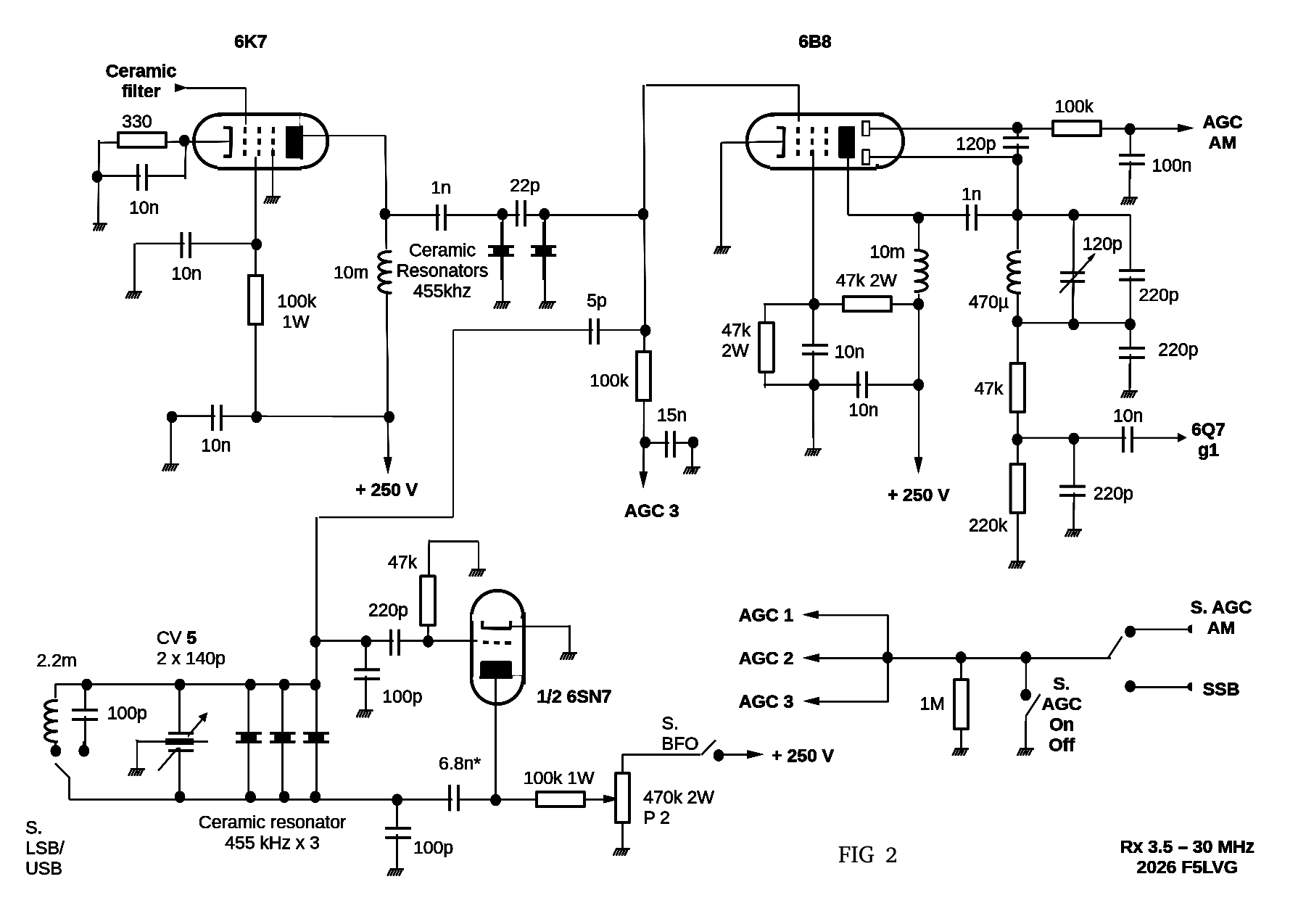
“Single-signal” selectivity is the ability of a receiver to pass only one side of the BFO frequency while rejecting the unwanted “image” signal on the opposite side of the desired signal.
Tubes: This stage uses a 6K7 and a 6B8.
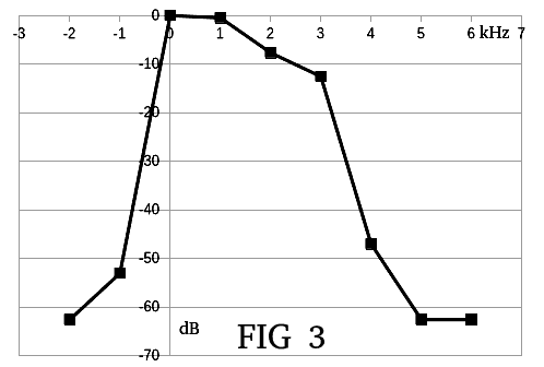
Input filter (selectivity): A bank of 10 ceramic resonators provides an ideal bandwidth for “Single Signal” SSB reception (Fig. 3).
Output filter: At the output of the 6K7, a second filter consisting of two ceramic resonators drives the 6B8.
AM and SSB detection (with the BFO): At the output, a tuned circuit is coupled to the two diodes of the 6B8 to provide demodulation and generate the automatic volume control (AVC) voltage in AM.
AGC: The AGC voltage is applied to both tubes (6K7 and 6B8).
Essential for SSB and Morse, it is built around one of the two triodes in a 6SN7.
Coupling: Very important with the first grid of the 6B8 tube.
USB / LSB switching: A group of three ceramic resonators in parallel, combined with the switching of a capacitor or inductor, shifts the frequency to switch instantly between Upper Sideband and Lower Sideband.
Adjustment: A variable capacitor allows fine adjustment of the pitch.
Note: The BFO plate voltage was made variable to optimize reception of weak signals, although this remains optional.
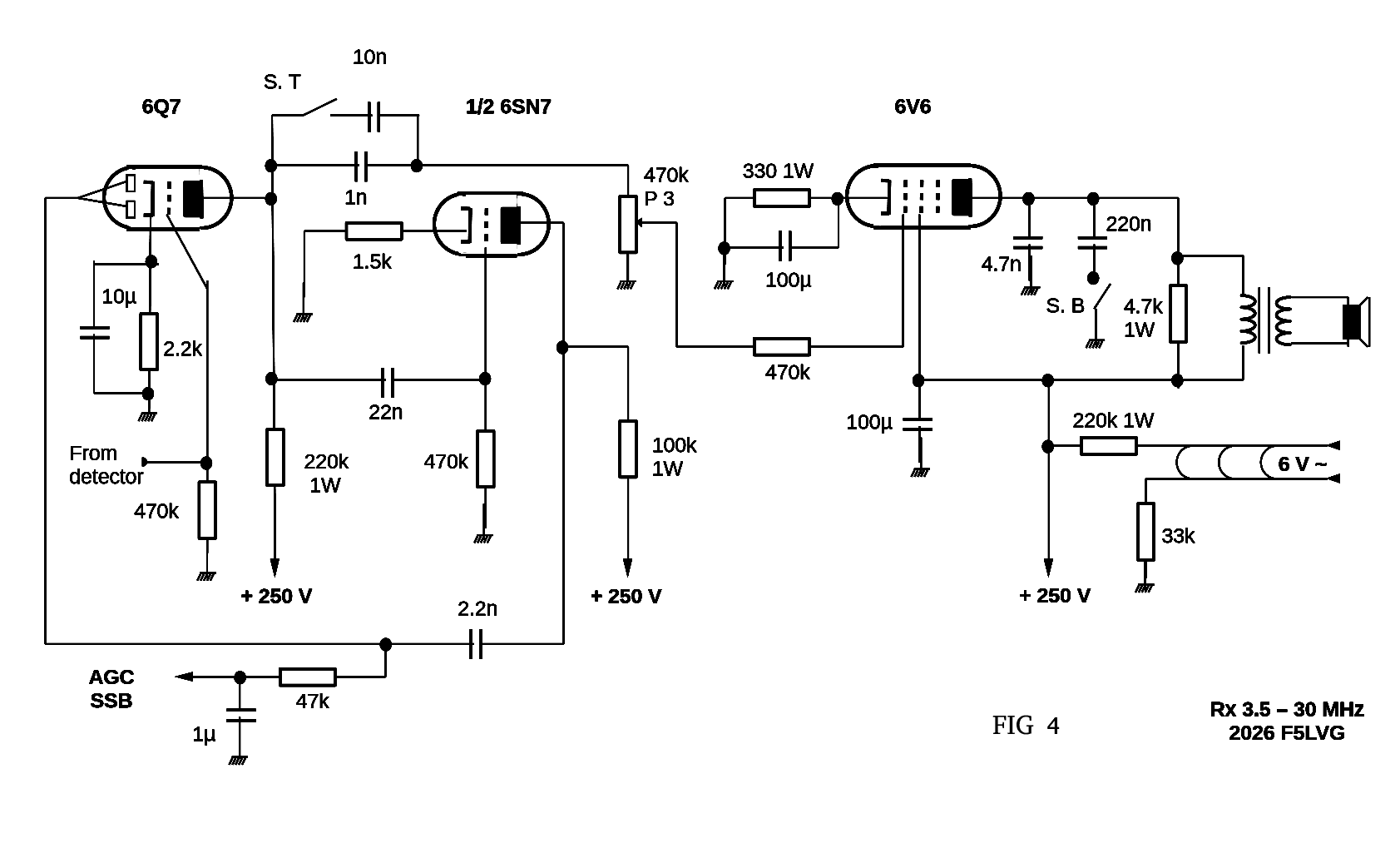
Audio chain: The demodulated signal is preamplified by the triode of a 6Q7 before driving the 6V6 power tube.
Tone control: A simple but effective system consisting of two switches and two capacitors.
AF-signal-based AGC circuit: This is the distinctive feature of this design for modern operating:
◦ At the output of the 6Q7, the audio signal is also fed to the second triode of the 6SN7.
◦ This triode amplifies the AF signal, which is then rectified by the diodes of the 6Q7.
◦ This produces a DC voltage proportional to the audio level, providing extremely effective AF AGC for SSB and Morse.
Switching:
◦ Switch 1 (S. AGC SSB AM): Selects the AGC source (IF AGC for AM, or AF AGC for SSB/CW).
◦ Switch 2 (S. AGC ON OFF): Completely disables the AGC (manual mode).
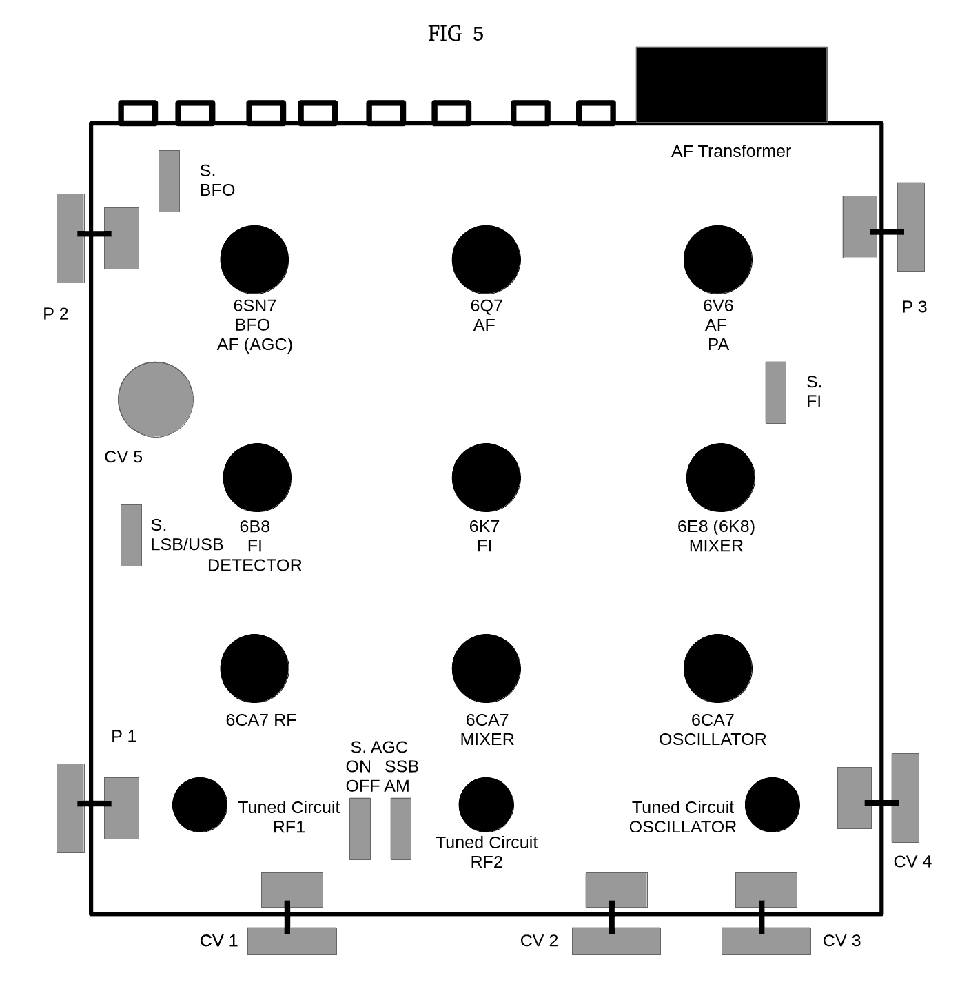
Practical Construction: Building Guide (Fig. 5)
The chassis is made from a wooden drawer measuring 29 × 29 × 8 cm.
Shielding and ground: Inside, the bottom, front panel and both side panels are lined with 5 cm-wide adhesive copper foil. The strips should overlap substantially to ensure excellent electrical contact.
Optimization: Add a few solder joints at the strip junctions to ensure minimum electrical resistance.
The design uses five small plastic variable capacitors rated 120/120/20/20 pF (part number 443DF).
Knob mounting: Insert M2.5x30 screws into the VC shafts to attach the control knobs easily. Caution: when tightening the screws, hold the shaft with pliers—not the body of the capacitor—to avoid damaging it.
Installation: The five variable capacitors are glued directly to the chassis using cyanoacrylate (superglue). Large-diameter knobs (A05 type) are recommended for easier tuning.
Following 1940s construction methods, the entire circuit is wired point-to-point. Insulated connection points are made using 10 MΩ (1 W) resistors as wiring supports.
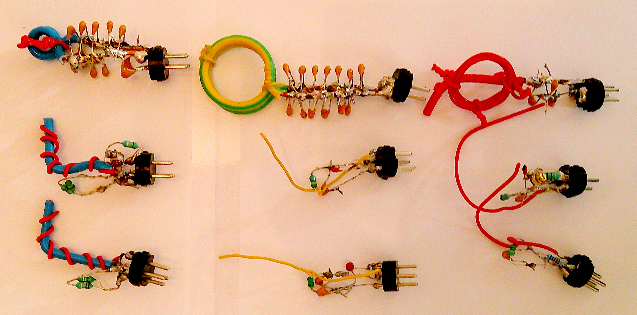
The tuned circuits of the RF stage and oscillator stage are built directly on DIN plug connectors. The coils and associated capacitors are mounted directly on them.
RF input (DIN 1): Built on a 3-pin plug.
RF output (DIN 2): Built on a 4-pin plug (this structural keying prevents confusion).
Components: For these first two modules, the coils are miniature inductors (about the size of an ordinary resistor). L1 and L2 must come from the same production batch so their values are as closely matched as possible.
For the oscillator tuned circuit, miniature inductors do not provide the required characteristics. The inductor must therefore be wound according to the operating frequency:
Above 10 MHz: Wind it using rigid 20 A installation wire (2.5 mm² cross-section).
Below 10 MHz: Wind it using 24 AWG single-strand wire.
Forming: Use everyday objects as temporary mandrels to obtain the required diameter: Noval tubes (22 mm), AA batteries (14 mm), or AAA batteries (11 mm). Wind the turns tightly around the mandrel, then remove the coil.
Support and rigidity:
◦ The turns are tightened and held in place with two small wires tied at the top and bottom of the coil.
◦ The 24 AWG coils are supported by a piece of rigid installation wire acting as a support.
Finishing: Solder the assembly to the DIN plug. Once alignment is complete, apply cyanoacrylate (superglue) to each coil to ensure the mechanical rigidity required for good frequency stability.
Oscillator capacitors: NP0 capacitors (with negligible temperature coefficient) are essential but difficult to source. The simplest solution is to purchase sets of multilayer ceramic NP0 capacitors from international marketplaces. By connecting several values in parallel, the exact required value can be obtained. Note that their voltage rating is generally 50 V.
Oscillator plate / tuned-circuit coupling capacitor: This is the most critical component in the design. It should have a relatively high value (4.7 to 10 nF, not critical) while withstanding a high voltage of 250 V.
The “vintage” SMD trick: For this coupling capacitor, use a 1210-size C0G SMD component rated at 500 V. Although large for an SMD part, it is still small. Simply solder a rigid wire to each end to turn it into a traditional axial-lead component that is easy to wire.
Practical Guide: Receiver Alignment and Optimization
The receiver’s final performance depends entirely on careful alignment. This delicate stage requires solid experience as well as a good theoretical and practical background.
Starting advice: Do not skip steps. Always begin testing on the 40-meter band (7.0 to 7.2 MHz), which is more forgiving.
Step 1: Setting the Oscillator Frequency Range (40 m)
The injection-frequency calculation varies according to the band:
Below 13 MHz: The oscillator operates above the receive frequency.
Above 13 MHz: The oscillator operates below the receive frequency.
Adjustment procedure:
Step 2: First Reception Tests (40 m) and RF Alignment
◦ Adjust the value of the antenna coupling capacitor on the first tuned circuit.
◦ Determine the value of the capacitor (or resistor) coupling the RF tube output to the second tuned circuit.
◦ Golden rule: The coupling must remain weak enough to prevent self-oscillation of the RF stage.
Step 3: Other Bands and Image-Frequency Rejection
Once the 40-meter band is properly aligned, you can move on to the other bands. As frequency increases, the adjustments become increasingly critical (oscillator stability and coupling sensitivity).
Sensitivity versus image-frequency rejection: A high L/C ratio increases receiver sensitivity, but also allows the image frequency to pass more easily.
Traps for the higher bands (from 21 MHz upward): It becomes necessary to add a dedicated series-tuned circuit to attenuate the image frequency. Tune the main variable capacitor (CV1) to the interfering image frequency, then adjust the trap capacitor until minimum noise is obtained (the attenuation null).
Results Obtained
The receiver was used with a 2 × 10 meter antenna:
DX performance: Excellent sensitivity. Japan, South Africa, Argentina, and many other distant countries were received in France. Across the spectrum, the antenna noise floor remains higher than the receiver’s own noise.
Frequency stability (SSB):
◦ Up to 14 MHz: Excellent stability for SSB reception after a short tube warm-up.
◦ At 18 and 21 MHz: Drift remains quite acceptable.
◦ At 24 and 28 MHz: A significantly longer warm-up period is required before stable reception is achieved.
Hand effect: Completely absent when operating the various capacitors.
AGC behavior: Very effective and responsive in SSB. It is, however, less effective in AM.
Tip for AM listeners: If you mainly listen to AM broadcast stations, you can widen the bandwidth of the 455 kHz IF filter by shorting out some of its input resonators, restoring treble to the audio.
DIN 1 / DIN 2 / DIN 3 Tuned Circuits
DIN 1 : L1=2,2µH / C1a=8pF / C1b=100pF
DIN 2 : L2=2,2µH / R2=4.7k / C2b=100pF
DIN 3 : L3 3 turns Ø=20mm / C3a=short-circuit / C3b=0pF / C3c=470+82+8+5pF
DIN 1 : L1=10µH / C1a=8pF / C1b=100pF
DIN 2 : L2=10µH / R2=22k / C2b=100pF
DIN 3 : L3 4 turns Ø=20mm / C3a et C3b = short-circuit / C3c=680+100+82pF
DIN 1 : L1=0.47µH / C1a=8pF / C1b=82pF
DIN 2 : L2=0.47µH / C2a=15pF / C2b=82pF
DIN 3 : L3 2 turns Ø=22mm / C3a et C3b = short-circuit / C3c=(100x10)+(33x2)+47pF
DIN 1 : L1=0.47µH / C1a=8pF / C1b=0pF
DIN 2 : L2=0.47µH / C2a=16pF / C2b=0pF
DIN 3 : L3 2 turns Ø=14mm / C3a=220pF / C3b=0pF / C3c=(100x9)+33+(30 adjustable)pF
DIN 1 : L1=1µH / C1a=8pF / C1b=0pF / Trap 4.7µH et 30pF adjustable in series
DIN 2 : L2=1H / C2a=6pF / C2b=0pF
DIN 3 : L3 2 turns Ø=11mm / C3a=short-circuit / C3b=82pF / C3c=(100x8)+90pF
DIN 1 : L1=0.47µH et 1µH en parallèle / C1a=8pF / C1b=0pF / Trap 4.7µH et 30pF adjustable in series
DIN 2 : L2=0.47µH et 1µH en parallèle / C2a=short-circuit / C2b=0pF
DIN 3 : L3 2 turns Ø=11mm / C3a=short-circuit / C3b=82pF / C3c=(100x4)+82+68+(30 adjustable)pF
DIN 1 : L1=0.47µH et 1µH en parallèle / C1a=8pF / C1b=0pF / Trap 4.7µH et 30pF adjustable in series
DIN 2 : L2=0.47µH et 1µH en parallèle / C2a=short-circuit / C2b=0pF
DIN 3 : L3 2 turns Ø=6mm / C3a=100pF / C3b=100pF / C3c=(100x6)+47+(30 adjustable)pF
DIN 1 : L1=470µH / R1=22k / C1b=68pF
DIN 2 : L2=10µH / C2a=0pF (stray capacitance of the plug) / C2b=68pF
DIN 3 : L3 19 turns Ø=20mm / C3a et C3b = short-circuit / C3c=0pF
Olivier ERNST F5LVG 2026
Figure captions:
Fig. 1: Receiver schematic: RF stage and frequency-conversion stages
Fig. 2: Receiver schematic: IF stages, BFO and demodulator
Fig. 3: IF-stage selectivity curve
Fig. 4: Receiver schematic: AF stages and SSB AGC
Fig. 5: Layout of the main components
Photo captions:
Photo 1: Receiver, top view
Photo 2: Receiver, bottom view
Photo 3: Interchangeable tuned circuits for the 10 m, 20 m and 80 m bands